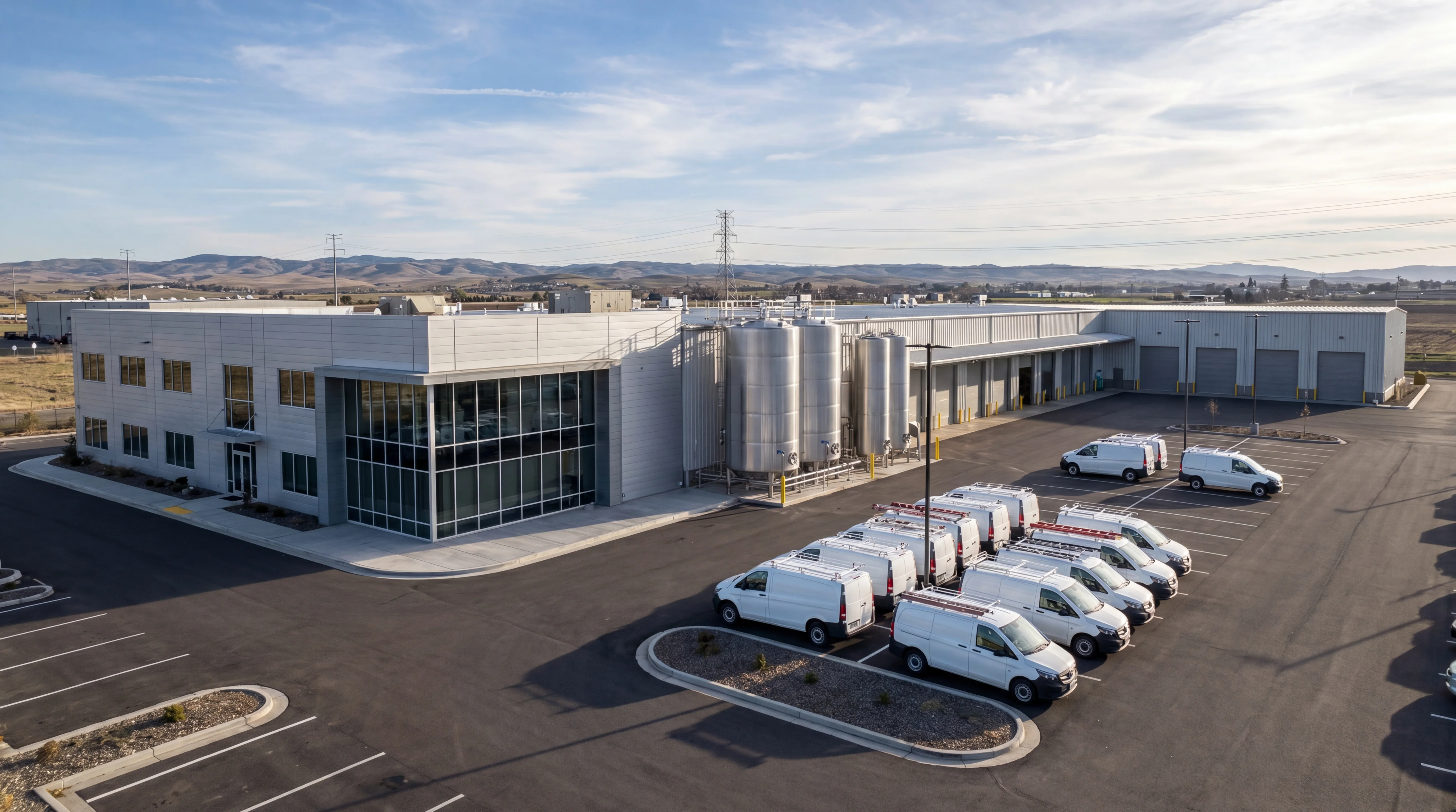
Precision Polishing Services Chicago
Micro-inch surface finishes at production scale for aerospace, medical, semiconductor, food-grade, and industrial parts.
1-business-day quotes ·ASTM, ASME BPE, SEMI F19, ISO 15730
Coverage at a glance
A single intake routes the part to the finishing facility with the right method, abrasive, and standard for the spec.
Polishing Services Covered
7 service lines spanning every common polishing method, finish grade, and substrate. Each is fulfilled by an accredited provider with the equipment for the part geometry and material.
Electropolishing Tier 1 · 9 methods covered
Electrochemical removal of microscopic surface peaks. Stainless and exotic alloys finished to ASTM B912-02, ASME BPE, SEMI F19, ASTM E1558, and ISO 15730, including citric and nitric acid post-dip passivation.
- ASTM B912-02 stainless steel electropolishing/passivation
- ASME BPE electropolishing (bioprocessing equipment)
- SEMI F19 semiconductor electropolishing
- ASTM E1558 metallographic electropolishing
- ISO 15730 stainless steel smoothing and passivation
- Anodic polishing (electrochemical polishing)
Mechanical Polishing Tier 1 · 6 methods covered
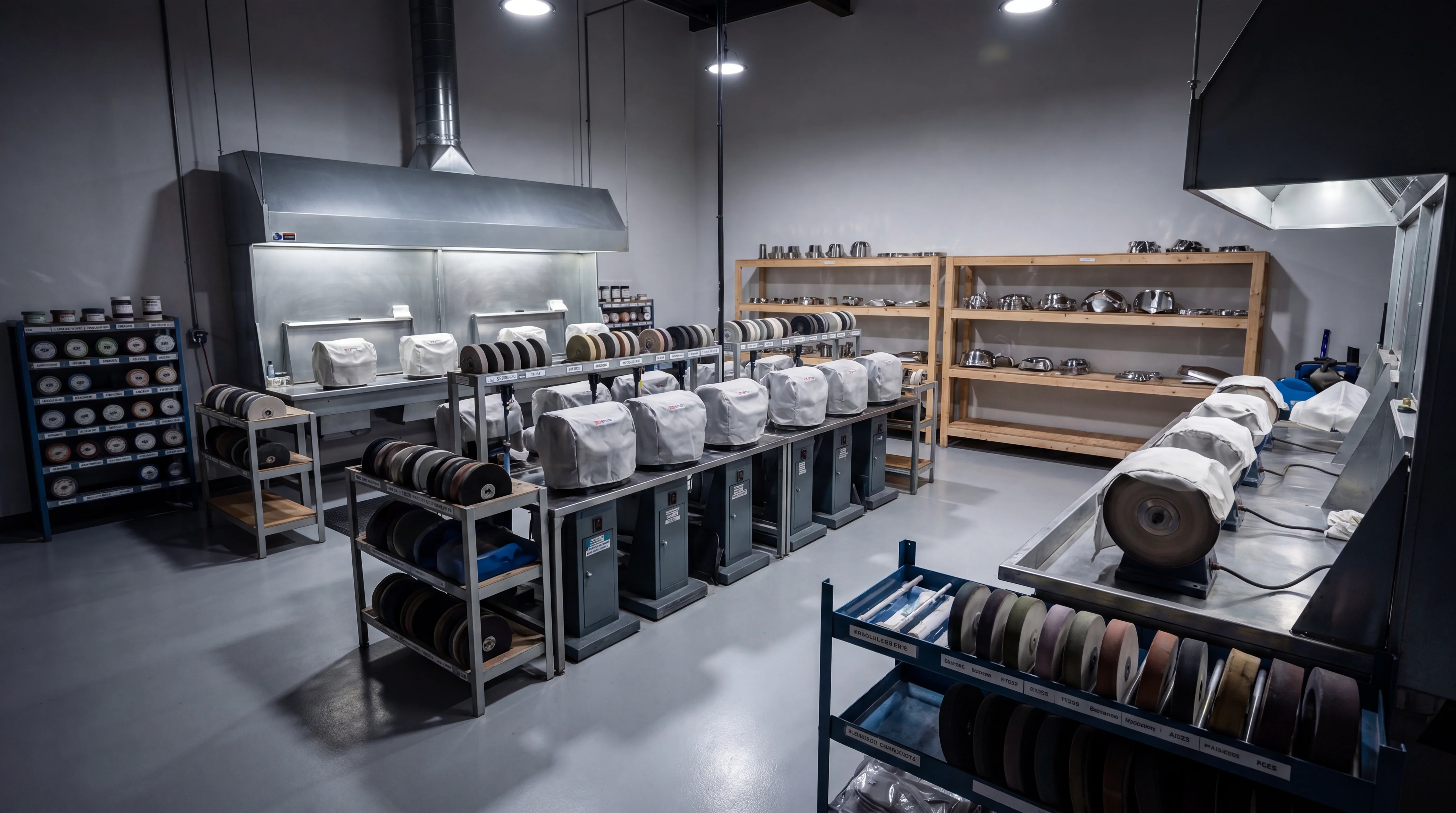
Rotary wheel, abrasive belt, buffing, and mechanical lapping operations refine bulk surfaces to specified Ra. Chemical-mechanical polishing (CMP) is supported for semiconductor and optical substrates.
- Chemical-mechanical polishing (CMP)
- Rotary polishing (wheel/belt machines)
- Belt polishing / abrasive belt grinding
- Buffing (cloth/soft wheel with polishing compound)
- Mechanical lapping
- Sandpaper / abrasive disc polishing
Face Polishing Tier 1 · 10 methods covered
Flat-face refinement using diamond and cerium-oxide abrasives. Mechanical, chemical, electro, vibratory, buffing, and abrasive-belt face polishing are covered, with silicon carbide and aluminum oxide abrasive paths.
- Diamond Abrasive Face Polishing
- Cerium Oxide Face Polishing (glass / optical)
- Mechanical Face Polishing
- Chemical Face Polishing
- Electropolishing (Electrochemical Face Polishing)
- Vibratory Face Polishing (Tumbling)
Stainless Steel Polishing Tier 1 · 4 methods covered
Mill (No. 1 / 2B), #4 brushed / directional / satin, No. 8 mirror, and low-gloss satin finishes for food, pharma, architectural, and industrial parts.
- Mill finish (No. 1 / 2B unpolished baseline)
- #4 brushed / directional / satin finish
- Mirror finish (No. 8)
- Satin finish (low-gloss, food/pharma)
Thread, Weld, and Assembly Polishing Tier 2 · 6 methods covered
Micro-abrasive thread lapping for tight-tolerance screws. Mirror weld blending, electrochemical TIG/MIG seam cleanup, flap-disc and non-woven abrasive finishing for fillet and corner welds.
- Thread Lapping (micro-abrasive precision screw lapping)
- Mirror Finish Weld Polishing
- Electrochemical Weld Cleaning / Polishing (TIG / MIG seams)
- Flap Disc Weld Blending
- Non-Woven Abrasive (Scotch-Brite-type) Weld Finishing
- Corner / Fillet Weld Polishing (cross / square / five-point access)
Sapphire Glass Polishing Tier 3 · specialty substrate
Flat and double-sided lapping plus precision polishing for sapphire windows, optical substrates, and watch crystals to optical-grade specifications.
View sapphire glass polishing specs →Silicon Wafer Polishing Tier 3 · specialty substrate
Chemical-mechanical polishing (CMP) for prime, test, epi, and SOI wafers, held to semiconductor flatness and surface roughness specifications.
View silicon wafer polishing specs →Tolerances Supported
Standard operating parameters across all polishing disciplines covered. Tighter specs are available on engineering review.
| Parameter | Max Variance |
|---|---|
| Surface Finish (Ra) | ≤ 1 µin |
| Flatness (Helium Light Bands) | 1 HBL |
| Parallelism | .000050" |
| Cylindricity | .000050" |
| Material Hardness Limit | 72 HRc |
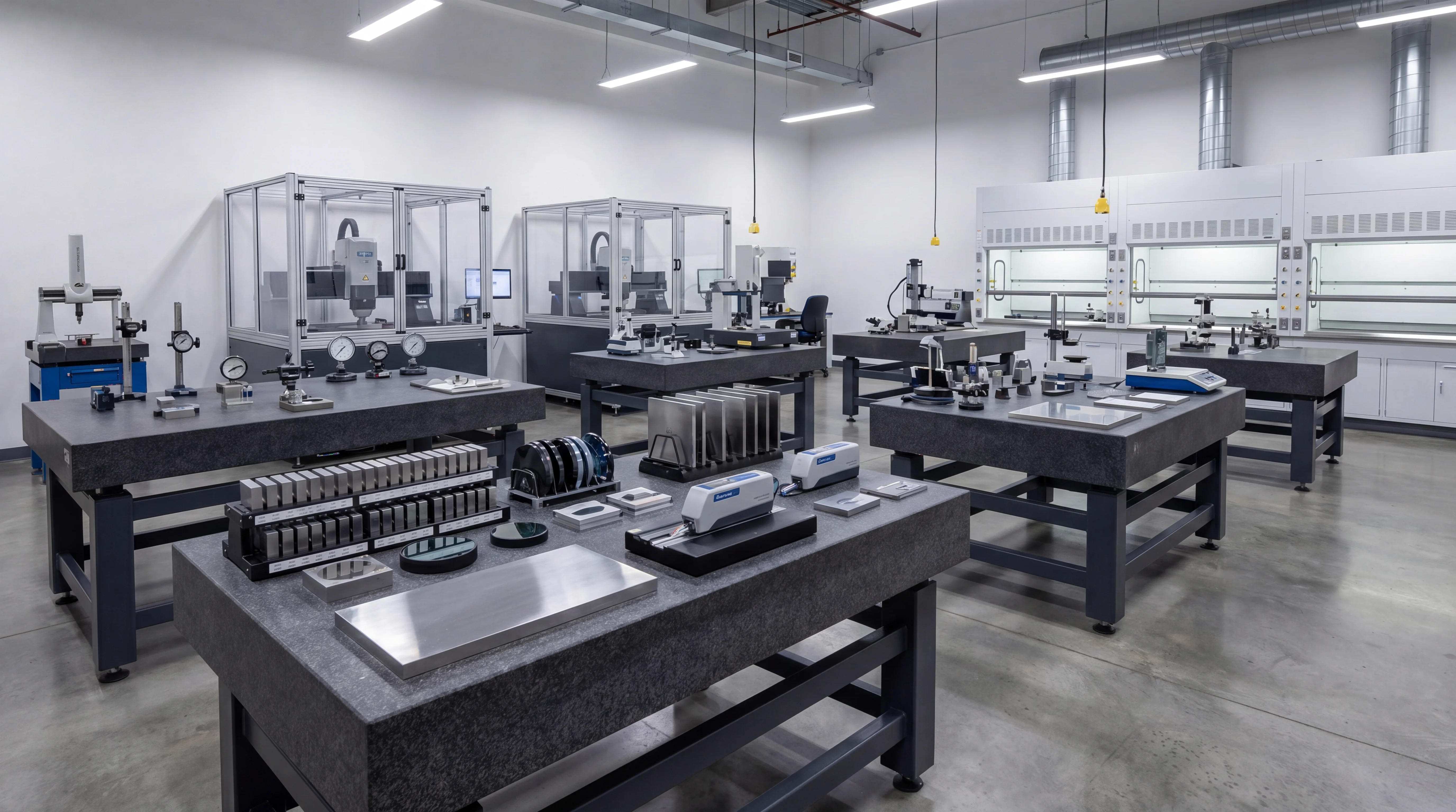
Process Flow
A standardized workflow for consistent, traceable results, applied across every service line and substrate.
Part Intake & Metrology
Incoming parts are logged and measured against baseline blueprints to determine required material removal and target Ra.
Method & Abrasive Selection
Compound grade, pad type, and machine kinematics are specified by an engineering review against the substrate, geometry, and finish standard (ASTM, ASME BPE, ISO 15730, SEMI F19).
Controlled Processing
Parts undergo controlled finishing loops (electropolishing, mechanical, CMP, vibratory, or vapor) with in-process profilometer spot checks to prevent over-polishing.
Final QA & Passivation
Final Ra and flatness readings are recorded, followed by multi-stage ultrasonic cleaning and (where specified) citric or nitric acid passivation.
Coverage Area
Polishing coverage spans the upper Midwest: Illinois, Wisconsin, Indiana, Michigan, and Iowa. Parts ship to an accredited finishing facility and return on a logged carrier. Each state below has a dedicated landing page with its city-level coverage.